- 您现在的位置:买卖IC网 > Sheet目录983 > HI5767EVAL1 (Intersil)EVALUATION PLATFORM HI5767
�� �
�
�HI5767EVAL1� Evaluation� Board� User’s� Manual�
�TM�
�Application� Note�
�January� 1999�
�AN9822�
�Description�
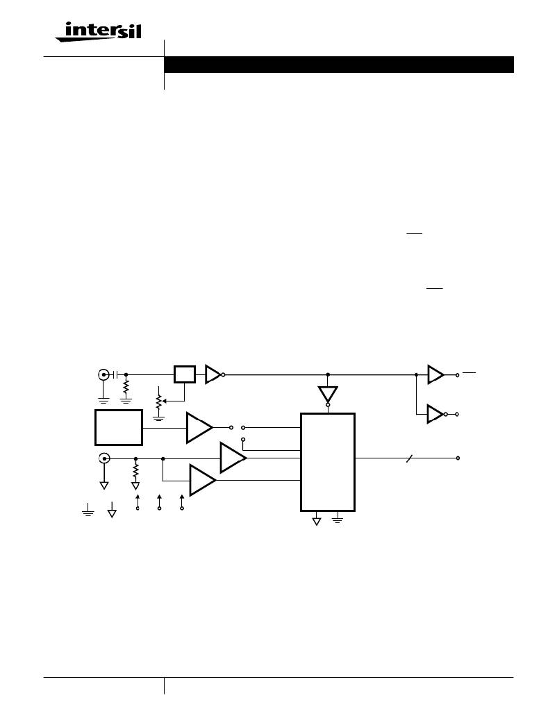
�The� HI5767EVAL1� evaluation� board� allows� the� circuit�
�designer� to� evaluate� the� performance� of� the� Intersil� HI5767�
�monolithic� 10-bit� 20/40/60MSPS� analog-to-digital� converter�
�(ADC).� As� shown� in� the� Evaluation� Board� Functional� Block�
�Diagram,� the� evaluation� board� includes� sample� clock�
�generation� circuitry,� a� single-ended� to� differential� analog�
�input� ampli?er� con?guration,� an� on� board� external� variable�
�reference� voltage� generator� and� a� digital� data� output�
�header/connector.� The� digital� data� outputs� are� conveniently�
�provided� for� easy� interfacing� to� a� ribbon� connector� or� logic�
�probes.� In� addition,� the� evaluation� board� includes� some�
�prototyping� area� for� the� addition� of� user� designed� custom�
�interfaces� or� circuits.�
�The� sample� clock� generator� circuit� accepts� the� external�
�sampling� signal� through� an� SMA� type� RF� connector,� J2.� This�
�input� is� AC-coupled� and� terminated� in� 50� ?� allowing� for�
�connection� to� most� laboratory� signal� generators.� In� addition,�
�the� duty� cycle� of� the� clock� driving� the� A/D� converter� is�
�Evaluation� Board� Functional� Block� Diagram�
�adjustable� by� way� of� a� potentiometer.� This� allows� the� effects�
�of� sample� clock� duty� cycle� on� the� HI5767� to� be� observed.�
�The� analog� input� signal� is� also� connected� through� an� SMA�
�type� RF� connector,� J1,� and� applied� to� a� single-ended� to�
�differential� analog� input� ampli?er.� This� input� is� AC-coupled�
�and� terminated� in� 50� ?� allowing� for� connection� to� most�
�laboratory� signal� generators.� Also,� provisions� for� a�
�differential� RC� lowpass� ?lter� are� incorporated� on� the� output�
�of� the� differential� ampli?er� to� limit� the� broadband� noise� going�
�into� the� HI5767� converter.�
�The� converters’� digital� data� outputs� along� with� two� phases�
�of� the� sample� clock� (CLK� and� CLK)� are� provided� at� the�
�output� header/connector.� With� this� output� configuration� the�
�digital� data� output� transitions� seen� at� the� I/O�
�header/connector� are� essentially� time� aligned� with� the�
�rising� edge� of� the� sampling� clock� (CLK)� or� the� falling� edge�
�of� the� out� of� phase� sampling� clock� (CLK).�
�Refer� to� the� component� layout� and� the� evaluation� board�
�electrical� schematic� for� the� following� discussions.�
�SAMPLE�
�CLOCK�
�INPUT�
�J2�
�50� ?�
�+5V� D�
�BIAS�
�TEE�
�CLK�
�CLOCK�
�OUT�
�1.2V�
�BANDGAP�
�VOLTAGE�
�VAR�
�GAIN�
�+2.5V�
�CLK�
�V� REFIN�
�CLK�
�REFERENCE�
�ANALOG�
�INPUT�
�J1�
�50� ?�
�G� =� +1�
�V� REFOUT�
�V� IN� +�
�D� 0� -D� 9�
�10�
�DIGITAL�
�DATA�
�OUT�
�G� =� -1�
�V� IN� -�
�(D0� -� D9)�
�DGND�
�AGND�
�HI5767�
�+5V� D�
�+5V� A�
�-5V� A�
�3-1�
�1-888-INTERSIL� or� 321-724-7143�
�|�
�Intersil� and� Design� is� a� trademark� of� Intersil� Corporation.�
�|�
�Copyright�
�?� Intersil� Corporation� 2000�
�发布紧急采购,3分钟左右您将得到回复。
相关PDF资料
HI5767EVAL2
EVALUATION PLATFORM HI5767
HI5805EVAL1
EVALUATION PLATFORM HI5805
HI5828EVAL2
EVALUATION PLATFORM HI5828
HI5960SOICEVAL1
EVALUATION PLATFORM SOIC HI5960
HI7188EVAL
EVALUATION PLATFORM HI7188
HI7190EVAL
EVALUATION PLATFORM HI7190
HJ4-L-DC12V
RELAY GEN PURPOSE 4PDT 5A 12V
HL2-HP-AC100V-F
RELAY GEN PURPOSE DPDT 10A 100V
相关代理商/技术参数
HI5767EVAL2
功能描述:数据转换 IC 开发工具 HI5767 HI FREQUENCY EVALUATION PLATFORM
RoHS:否 制造商:Texas Instruments 产品:Demonstration Kits 类型:ADC 工具用于评估:ADS130E08 接口类型:SPI 工作电源电压:- 6 V to + 6 V
HI5780
制造商:INTERSIL 制造商全称:Intersil Corporation 功能描述:10-Bit, 80 MSPS, High Speed, Low Power D/A Converter
HI5780-EV
制造商:INTERSIL 制造商全称:Intersil Corporation 功能描述:10-Bit, 80 MSPS, High Speed, Low Power D/A Converter
HI5780JCQ
制造商:Rochester Electronics LLC 功能描述:32 PQFP COMTEMP VIDEO D/A 10BIT 80MHZ - Bulk 制造商:Harris Corporation 功能描述:
HI5780JCQ-T
制造商:Rochester Electronics LLC 功能描述:HI5780JCQ IN TAPE & REEL - Bulk
HI5800
制造商:INTERSIL 制造商全称:Intersil Corporation 功能描述:12-Bit, 3MSPS, Sampling A/D Converter
HI5800_00
制造商:INTERSIL 制造商全称:Intersil Corporation 功能描述:12-Bit, 3MSPS, Sampling A/D Converter
HI5800BID
制造商:INTERSIL 制造商全称:Intersil Corporation 功能描述:12-Bit, 3MSPS, Sampling A/D Converter